| BORon nitride as heat spreader On GAN HEMT RF transistors |
Performances of electronic devices & systems are drastically impacted by thermal issues
Classical cooling solutionThe most classical solution today is to use the packaging stack. The efficiency of this solution depends on the distance from the heat source. The main disadvantage is that the heat is spreading into the component structure, and may cause some damages.BoroGaN project cooling studyA nanocrystalline Boron Nitride (BN) thin film deposited on top of a Gallium Nitride-based (GaN) transistor, in the closest vicinity of the active zone, where the heat is generated. This approach should improve drastically the efficiency of dissipated power removal, as this nano-structured material has a much improved thermal conductivity in the z-axis compared with its nominal counterparts.Application to High Electron Mobility TransistorsThe High Electron Mobility Transistors (HEMTs) are subject to intense current densities and high electric fields (several MV/cm). During operation, the estimated temperature of the channel increases significantly. | 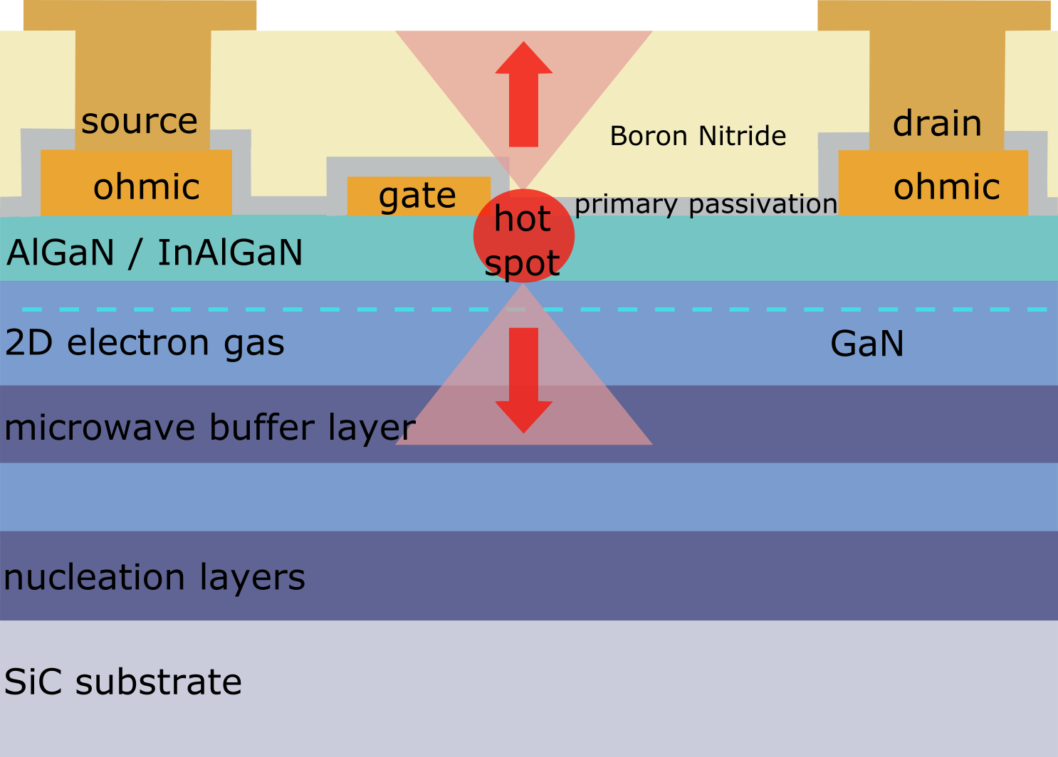 Schematics of heat flow in a HEMT device with top heat spreader |
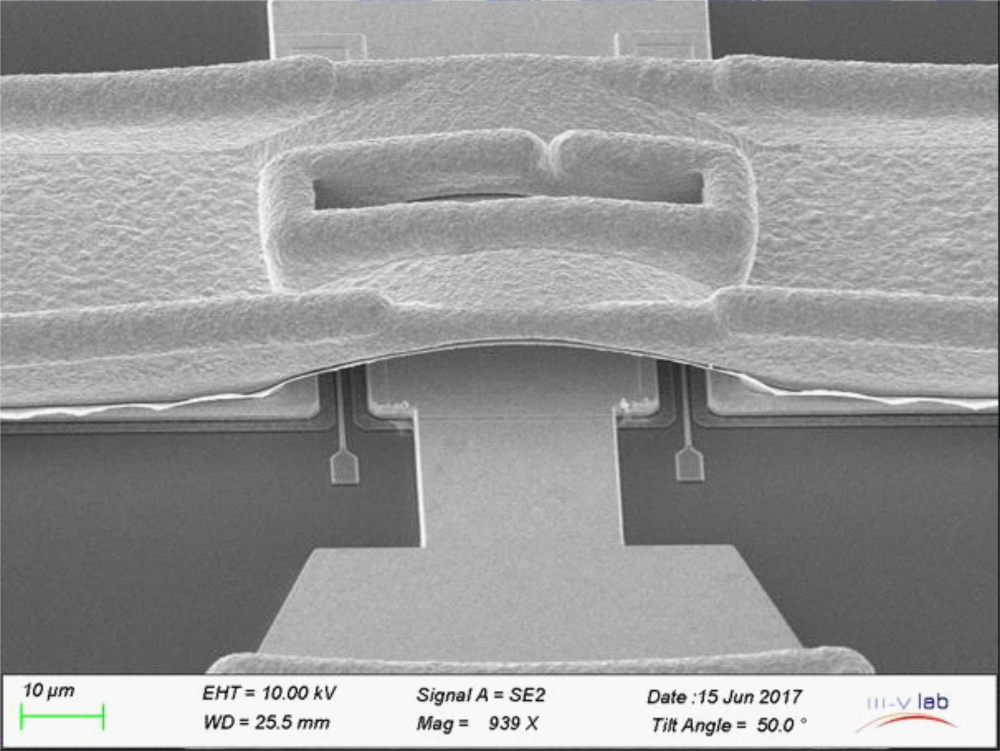 GaN HEMT Transistor for Microwave Applications (III-V Lab) |
A reduction of the operating temperature by 35°C would lead to more than tenfold device lifetime improvement.
Moreover the BN shows suitable physical properties for heat spreader with a high thermal conductivity, a high breakdown electric field, and a high electrical resistivity. The last parameter is important to give rise to low microwave losses up to 60 GHz.
Planned studiesA new technological building block based on high thermal conductivity BN will be developed, which will be compatible with microelectronics processes. The BN deposition technique will allow room temperature deposition, i.e. will be compatible with the other technological steps.Work programThe first work package is devoted to the growth, optimization and characterization of BN thin films on various substrates at NTU. III-V Lab will fabricate specific elementary devices as MIM structures for electrical BN characterisation.The second work package is dedicated to the application of BN thin films for the GaN HEMT heat-spreader. III-V Lab will elaborate GaN-based heterostructures and microwave transistors to allow the growth of BN on top of devices. These transistors will be characterised through static, dynamic and load-pull measurements. Finally, the devices will be characterised thermally during operation with the thermoreflectance technique by CNRS. This non-contact optical method shows excellent spatial resolutions of the order of 200–500 nm. The thermal resistance values for the structures with and without BN heatspreader will be measured and compared. |